Advanced Ceramics for the Semiconductor Industry
How can precision and reliability in semiconductor production be continuously increased? Which materials can withstand the extreme conditions in chip production? With over 120 years of experience in technical ceramics, we supply you with customised high-performance components for the semiconductor industry. Whether for wafer processing, production or handling - our ceramic solutions made of Al₂O₃, AlN, SiSiC and Si₃N₄ impress with the highest purity, thermal stability and mechanical precision. Also discover how hermetic feedthroughs enable vacuum tightness, high purity and minimised particle formation.
Key Facts at a Glance
- CeramTec supplies high-performance ceramics made from Al₂O₃, AlN, SiSiC, and Si₃N₄ for wafer processing, chip manufacturing, and wafer handling.
- Achievable manufacturing precision: flatness < 1 μm, roughness Ra ≥ 0.05 μm – suitable for EUV lithography and CVD/PVD processes.
- Complete development partner: from material consulting and prototyping through to ISO Class 5-certified series production.
Indispensable for the Semiconductor Business
Whether in wafer processing, semiconductor manufacturing or handling - our components made of high-performance ceramics enable long-lasting performance and reliability.
CeramTec offers the right ceramic material for almost every requirement:
- Al₂O₃ – high purity and rigidity
- AlN – high thermal conductivity and electrical insulation
- SiSiC – low thermal expansion and density
- Si₃N₄– high fracture toughness and low thermal expansion
Based on individual requirements, we can recommend the optimum material selection for the customer application. We are continuously improving key steps in our manufacturing process while simultaneously expanding our production capabilities.

What Manufacturing Precision does CeramTec achieve for Ceramic Semiconductor Components?
| KEY PROCESS STEPS | TECHNICAL PARAMETERS | REACHABLE VALUES/REQUIREMENTS |
| Hard machining - milling | Flatness, parallelism, Ra | Flatness < 1 μm Ra ≥ 0,05 μm" |
| Grinding | Flatness | 5 μm < Ø 200 mm / 10 μm > Ø 200 mm |
| Parallelism | 5 μm < Ø 200 mm / 10 μm > Ø 200 mm | |
| Roughness | Ra from 0,15 μm to 0,6 μm | |
| Eroding | Symmetrical positioning | up to 0,05 mm (holes/grooves positioning) |
| Lapping & polishing | Flatness, parallelism, Roughness | Ra from 0,06 μm to 0,35 μm Flatness < 2 μm Parallelism < 2 μm |
| Structuring | Roughness | Roughness < 3,2 μm Size < 150 μm |
| Special measurement | Local slope/local flatness | Objective resolution 50 nm - 25 μrad |
| Cleaning & packaging | Cleanliness | ISO 5 / Clean room 100 / package in clean room (based on customer request) |
Customized Advanced Ceramic Solutions
We manufacture our ceramic components and parts according to your individual application requirements, so you can design and maintain your processes flexibly and reliably. We have transitioned from a manufacturer of high quality ceramic components to a strong development partner who transforms your individual requirements into state of the art semiconductor products.
- Basic Suitability of Ceramics
- Selection of Materials
- Tailored Design & Construction
- Prototypes
- Risk Management
- Simulating and Modeling
- Specification
- Quality Assurance
- Series Production
- Change Management
- Audits
- Product Training
- Application Training
- Further Development and Know-How Transfer
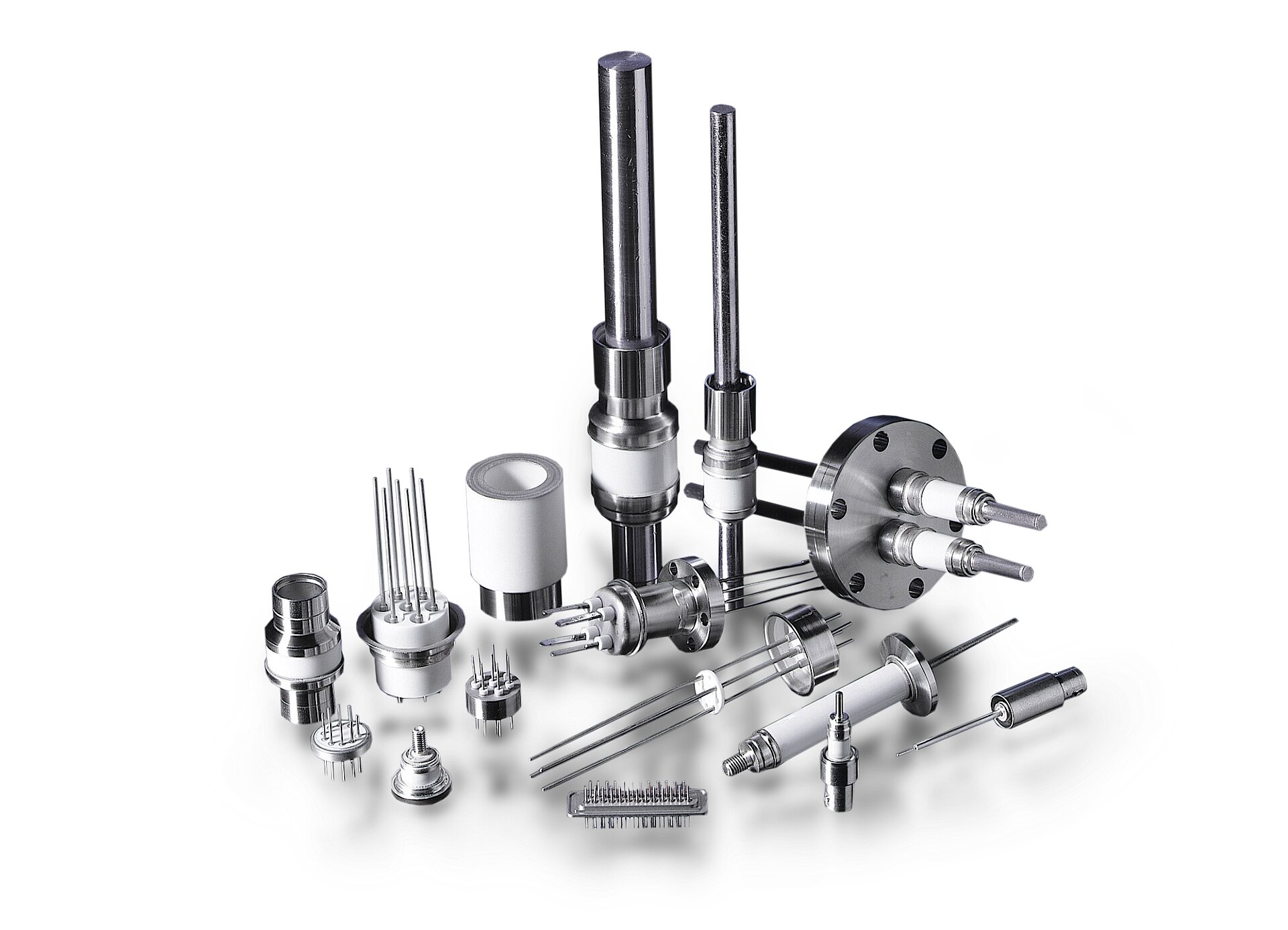
Hermetic Assemblies
Also discover our hermetically sealed, ceramic-metallic Ceramaseal® connections from our team at CeramTec North America CTNA. They enable vacuum tightness, high purity and minimised particle formation, properties that are crucial for vacuum processes in semiconductor production. They therefore act as a safe interface in low-oxygen and demanding semiconductor environments.
FAQ - CeramTec Semiconductor Business
What role do technical ceramics play in the semiconductor industry?
- High temperature resistance: Many processes in chip production take place at very high temperatures. Technical ceramics retain their dimensional stability and properties even under these conditions.
- Chemical resistance: Aggressive gases and liquids are used in etching, deposition and cleaning processes. Ceramics are extremely resistant to corrosion and do not react with these media.
- Electrical insulation: Many ceramics are excellent electrical insulators, which is crucial for the precise control of electrical currents and the prevention of short circuits in complex circuits.
- High hardness and wear resistance: Components are often subjected to mechanical stress and must be extremely abrasion resistant to ensure a long service life and process stability.
- Low thermal expansion: Low thermal expansion is important to ensure dimensional stability and precision during temperature fluctuations.
- High thermal conductivity (for certain applications): Certain ceramics, such as aluminium nitride, dissipate heat very well, which is essential for thermal management in high-performance applications.
- Vacuum resistance: As many semiconductor processes take place in a vacuum, the materials used must be vacuum-compatible.
What materials does CeramTec use for semiconductor applications?
CeramTec offers a variety of high-performance ceramics relevant to the semiconductor industry, including
- Aluminium oxide (Al2O3): Excellent electrical insulation, high hardness and chemical resistance. CeramTec offers Rubalit®, for example.
- Aluminium nitride (AlN): Particularly important due to its high thermal conductivity combined with excellent electrical insulation. CeramTec offers a corresponding product in the form of Alunit®.
- Silicon carbide (SiC): High hardness, wear resistance, high temperature resistance and good thermal conductivity. CeramTec offers ROCAR® and focusses on process integration in the manufacture of SiSiC plates for semiconductor machines.
- Silicon nitride (Si3N4): High strength, fracture toughness and good thermal shock resistance. CeramTec offers Sinalit®, for example.
- Zirconium oxide (ZrO2): High fracture toughness and wear resistance.
For which applications are CeramTec components used in semiconductor production?
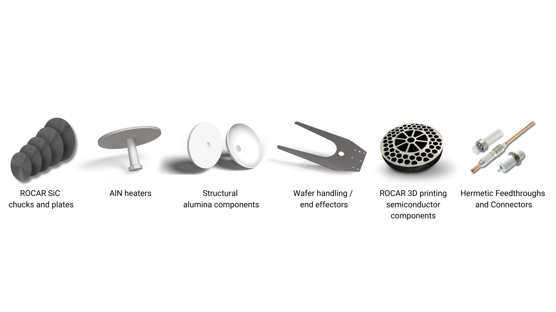
- Wafer handling: Components such as wafer chucks (holders for wafers), gripper arms and end effectors that move the delicate wafers without damaging them.
- Process chamber components: Liners, gas manifolds, nozzles and other internal components in process chambers for deposition, etching and diffusion processes.
- Heating and cooling systems: Ceramic heating plates or heat sinks for precise temperature control during the various manufacturing steps.
- Electrical insulators and feedthroughs: Wherever electrical insulation is required at high temperatures and under aggressive conditions.
- Substrates for electronic circuits: Ceramic substrates serve as carriers for electronic components and provide high heat dissipation and electrical insulation.
- Optical components: High-precision ceramic components can be used in lithography and inspection systems.
